With Numerous Citations, Harshitkumar J. Ghelani is Revolutionizing PCB Manufacturing Through AI and Process Optimization
The integration of Artificial Intelligence (AI) and data-driven analytics is reshaping the way printed circuit boards (PCBs) are manufactured. Harshitkumar J. Ghelani, a distinguished engineer with over nine years of experience in process optimization and quality control, has been at the forefront of this transformation. His extensive work focuses on automating the detection of flaws, improving electroplating techniques, and raising the overall efficiency of production. These are all very important in an industry that is being driven more and more by miniaturization and the need for high-precision electronics.
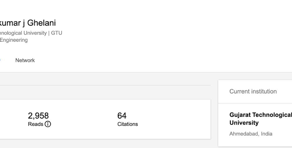
Ghelani’s research portfolio has garnered significant attention, reflected in his ResearchGate score of 65.6, 64 citations, and over 2,958 reads—a testament to the impact of his contributions. Through rigorous experimentation and field-validated insights, he has demonstrated how AI can address both long-standing and emerging challenges in PCB manufacturing.
In his research paper titled “AI-Driven Quality Control in PCB Manufacturing: Enhancing Production Efficiency and Precision,” Ghelani explores how machine learning, computer vision, and predictive analytics outperform traditional inspection methods, including manual checks and Automated Optical Inspection (AOI). By analyzing defects in real time and predicting potential failure points, AI-driven systems significantly reduce human error, cut operational costs, and accelerate the overall production timeline. This advanced quality-control framework also ensures compliance with industry standards. establishing new benchmarks for cost-effective, high-precision manufacturing. Following a thorough peer review, Ghelani’s manuscript was officially accepted by the International Journal of Scientific Research and Management (IJSRM), highlighting his expertise. In under six months, the article has already received 64 citations worldwide, as documented on his
Ghelani has also addressed persistent issues like void formation in his “Root Cause Analysis for Void and Minimized Production Defect” initiative. In 2019, void-related defects led to the rejection of 10,496 PCBs—a costly problem that risked delaying orders and undermining client confidence. By implementing a detailed void identification guide and systematic improvements, Ghelani successfully reduced the rejection rate by 90% within two years. This achievement underlines the importance of data-driven defect tracking, interdepartmental collaboration, and real-time process monitoring in preventing large-scale product failures.
Another area where Ghelani has made a significant contribution is in optimizing electroplating for uniform current distribution. His redesigned rectifier circuit, which delivers a stable and near-linear DC output, not only resolved ripple-induced defects but also drove down the annual scrap rate from 70% to 10%. These process refinements cut rejection rates from 20,000 boards per year to 2,500 and showcased how precise circuit optimization can lead to dramatically improved yield, lower costs, and better product consistency.
Currently serving as a Process Project Designer at H and T Global Circuit Factory LLC, Ghelani applies his deep expertise in PCB fabrication, micro cross-section analysis, AS9102 First Article Inspection (FAI), and advanced testing methodologies. His previous roles at SMG-Global Circuits, Inc. and GRIM TECH Project Pvt. Ltd. fortified his competence in international compliance standards, supplier quality management, and process troubleshooting. Beyond research, he plays a pivotal role in mentoring teams, enhancing manufacturing workflows, and implementing automation to achieve higher productivity and reduced defect rates.
As AI, automation, and advanced analytics continue to shape the future of electronics manufacturing, Ghelani’s work exemplifies a forward-looking approach. By combining academic research with hands-on engineering, he is charting a path toward more efficient, scalable, and reliable PCB production. His leadership in integrating AI-driven quality control, minimizing defects, and optimizing plating processes has already set new standards in the industry. Through his numerous citations and continuous innovation, Harshitkumar J. Ghelani stands as a key figure guiding PCB manufacturing into the next era of technological excellence
Media Contact
Company Name: CB Herald
Contact Person: Ray
email: ray@cbherald.com
Country: USA